 entrance
Using a charger as a power supply. How to remake the charger from the cell phone to another voltage
On the Internet you can meet alternative ways of using the ballasts of energy-saving lamps. This article will consider the option of making a pulsed power supply unit for charging a mobile phone. The block is able to provide a sufficiently large current at the output (up to 1 amp), which will allow you to apply it to charge mobile devices. The power supply is working silently, overheating did not notice.
The device can be manufactured in a few minutes. To begin with, you need to fall out the duty transformer from the non-working computer power supply. Further simpler simple. The voltage at the outlet of the ballast is about 1000 volts, through a non-polar capacitor, the voltage is fed to the transformer. At the output of the transformer, you can get several different stresses, only 5-6 volts will be enough for charging.
The output voltage is quite high frequency, therefore, for straightening, pulse diodes should be used, for example, FR107 / 207 or similar.

As a container, you can use any electrolytic capacitor from 100 to 1000 μF, a voltage from 10 to 25 volts (no longer makes sense).
Photo images can be easily navigated with a ballast alteration scheme.

Carefully look at the transformer from the computer power supply. On both sides, we see contacts. If you look at the top, then we can see 3 contacts on the left, to two extremes supply voltage from the ballast, the average contact is left free.

At the output of the transformer, after the diode you can use Stabilitron at 5.5-6 volts, although it can be excluded, since the output voltage is not much "floats"

The scheme uses a non-polar capacitor 1000-3300mkf, voltage 3 ... 5 kV. The device can be placed in the housing from the factory charger for the mobile phone. As far as such a device will work, unfortunately, I can not answer, but it already works for 3 days, even left the ones on the night.
List of radio elements
| Designation | A type | Nominal | number | Note | Score | My notebook |
|---|---|---|---|---|---|---|
| T1, T3. | Bipolar transistor | MJE13003. | 2 | In notebook | ||
| T2, T4. | Bipolar transistor | FJA13009 | 2 | In notebook | ||
| VD1-VD9 | Rectifying diode | FR107. | 9 | In notebook | ||
| VD10 | Stabilirton | 1 | In notebook | |||
| VDS1, VDS2. | Rectifying diode | 1N4007. | 8 | In notebook | ||
| C1, C2, C7, C8 | 1 μF | 4 | In notebook | |||
| C3, C9. | Capacitor | 2200 PF | 2 | In notebook | ||
| C4. | Capacitor | 0.047 MKF. | 1 | In notebook | ||
| C5. | Capacitor | 10 NF | 1 | In notebook | ||
| C6, C12 | Electrolytic condenser | 10 μF 400 in | 1 | In notebook | ||
| C10 | Capacitor | 2200 PF 3-5 kV | 1 | In notebook | ||
| C13. | Electrolytic condenser | 1 | In notebook | |||
| R1, R2, R7, R8 | Resistor | 24 Oh. | 4 | In notebook | ||
| R3, R6, R9, R12 | Resistor | 510 com | 4 | In notebook | ||
| R4, R5, R10, R11 | Resistor | 33 Oh. | 4 |
Power supply - from a cell phone charger
I. Nechaev, Kursk
The small-sized wear apparatus (radio receivers, cassette and disk players) are usually designed for food from two to four galvanic elements. However, they serve for a long time, and they have to be replaced quite often with new ones, so at home this equipment is advisable to feed from the mains block. Such a source (in the spaciousness is called the adapter) It is not difficult to purchase or make it, the benefit in the amateur literature is a lot of them. But you can do and otherwise. In almost three out of every four inhabitants of our country today there is a cell phone (according to the research company AC & M-Consulting, at the end of October 2005. The number of cellular subscribers in the Russian Federation exceeded 115 million). Its charger is used for a direct purpose (to charge the phone's battery) for only a few hours a week, and the rest of the time is inactive. On how to adapt it to power the small equipment, it is described in the article.
In order not to spend money on the electroplating elements, the owners of wearable radio receivers, players, etc. The equipment use batteries, and in stationary conditions they feed these devices from the AC network. If there is no finished power supply with the desired output voltage, it is not necessary to buy or collect such a block itself, you can use a charger from a cell phone that many people today have.
However, it is impossible to directly connect it to the radio or player. The fact is that most of the chargers included in the cellular telephone pack are a non-bilized rectifier, the output voltage of which (4.5 ... 7 V with a load current 0.1 ... o, for) exceeds the required for power to power apparatus. The problem is solved simply. To use the charger as a power supply, it is necessary to turn on the voltage adapter-stabilizer between it.
As the name itself says, the basis of such a device should be a voltage stabilizer. It is most convenient to collect on a specialized microcircuit. The large nomenclature and availability of integral stabilizers allow you to make a variety of options for adapters.
The schematic diagram of the voltage stabilizer is shown in Fig. 1. Chip DA1 choose 
depending on the required output voltage and current consumed. The capacitance of C1 and C2 capacitor can be in the range of 0.1 ... 10 MCF (rated voltage - 10 V).
If the load consumes up to 400 mA and such a current is able to pay the charger, as DA1, the KR142En5A chips (output voltage - 5 V), KR1158ENZV, KR1158ENZG (3.3 V), KR1158NEn5V, CR1158H5G (5 V), and Pytyatolet Imported 7805, 78m05. The chips of the LD1117XXXXXXX series are also suitable, REG 1117-XX. Their output current - up to 800 mA, output voltage - from a number of 2.85; 3.3 and 5 V (in LD1117XXXX - also 1.2; 1.8 and 2.5 V). The seventh element (letter) in the designation LD1117XXXXXX indicates the type of housing (S - Sot-223, D - S0-8, V - TO-220), and the two-digit number followed by it - on the nominal value of the output voltage in tenth voltage (12 - 1.2 V, 18 - 1.8 V, etc.). The number attached through a hyphen in the designation of the REG1117-XX microchip also indicates stabilization voltage. The basement of these chip in the SOT-223 housing is shown in Fig. 2, a.
It is permissible to use and chip stabilizers with adjustable output voltage, for example, KR142EN12A, LM317T. In this case, you can get any value of the output voltage from 1.2 to 5 ... 6 V.
With the nutrition of equipment that consumes a small current (30. .100 mA), for example, a small-sized VHF of the Cup of radio receivers, in the adapter, you can apply chips KR1157EN5A, kr1157en5b, kr1157en501a, kr1157en501b, kr1157en502a, kr1157en502b, kr1158en5a, kr1158en5b (all with nominal output voltage 5 V ), Kr1158Enza, kr1158enzb (3.3 V). Drawing of a possible version of the printed circuit board with
the use of the latter series chips is shown in Fig. 3. Capacitors C1 and C2 - small-sized oxide of any type of 10 μF capacity.
It is possible to significantly reduce the size of the adapter, using the LM3480-XX miniature chips (the last two digits indicate the output voltage). They are produced in the SOT-23 housing (see Fig. 2.6). The drawing of the printed circuit board for this case is depicted in fig. 4. Capacitors C1 and C2 - small-sized ceramic K10-17 or similar imported with a capacity of at least 0.1 μF. The appearance of adapters mounted on boards made in accordance with Fig. 3 and 4 are shown in Fig. five. 
It should be noted that the foil on the board can perform the function of the heat and removal. Therefore, the conductor area under the withdrawal of the chip (common or output) through which heat is carried out, it is advisable to make as much as possible.
The collected device is placed in a plastic box of suitable sizes or into the battery compartment of the apparatus. For docking with the charger, the adapter must be provided with an appropriate outlet (similar to the one that is installed in the cell phone). It can be placed on a printed circuit board with a stabilizer or fasten on one of the walls of the box.
Establishing an adapter does not require, you only need to check it in working with connecting wires that will be used to connect to the charger and the feeder. Self-excitation is eliminated by an increase in the capacitance of C1 and C2 capacitors.
LITERATURE
1. Biryukov C. Microchipped voltage stabilizers wide use. - Radio, 1999, No. 2, p. 69-71.
2. LD1117 Series. Low Drop Fixed and Adjustable Positive Voltage Regulators. -
3. REG1117, REG1117A. 800mA and 1a Low Dropout (LDO) Positive Regulator 1.8V, 2.5V, 2.85V, 3.3V, 5V and Adjustable. -
4. LM3480. 100 MA, SOT-23, Quasi Low-Dropout Linear Voltage Regulator. -
Most modern network chargers are assembled along the simplest pulse scheme, on one high-voltage transistor (Fig. 1) according to the block generator scheme.
In contrast to simpler diagrams on a reduced 50 Hz transformer, the transformer in the pulse converters of the same power is much smaller in size, and therefore less dimensions, weight and price of the entire converter. In addition, the pulse transducers are more secure - if the conventional converter has a high unstable (and sometimes variable) voltage from the secondary transformer winding, then with any malfunction of the "pulse" (except for the failure of the inverse Communications - but it is usually very well protected) at the output there will be no voltage at all.

Fig. one
Simple Pulse Block Generator Scheme
For a detailed description of the principle of operation (with pictures) and calculating the elements of the diagram of a high-voltage pulse converter (transformer, capacitors, etc.), you can read, for example, in the "TEA152X Efficient Low Power Voltage Supply" view http: // www. nxp.com/acrobat/applicationnotes/an00055.pdf (in English).
The variable network voltage is straightened by the VD1 diode (although sometimes generous Chinese put four diodes, over a bridge circuit), current pulse when turned on is limited to the R1 resistor. It is advisable to put a 0.25 W resistor to put a resistor - then during overload it burns, performing the fuse function.
The converter is assembled on the VT1 transistor according to the classic reverse scheme. The R2 resistor is needed to start generation when powering, in this scheme it is optional, but the converter works with it a little more stable. Generation is supported by the C1 condenser included in the PIT circuit on the winding the generation frequency depends on its tank and transformer parameters. When removing the transistor, the voltage on the lower under the diagram of the outputs of the windings / and II is negative, on the upper - positive, positive half-wave through the C1 condenser, the transistor opens the transistor, the voltage amplitude in the windings increases ... That is, the transistor is avalanche-like opens. After some time, as the C1 capacitor charge, the base current begins to decrease, the transistor begins to close, the voltage on the top according to the scheme of the winding of the winding II begins to decrease, through the C1 condenser, the base current decreases even more, and the transistor is avalanche-like closed. The R3 resistor is needed to limit the base current when overloading the circuit and emissions in the AC network.
At the same time, the amplitude of the self-induction EMF through the VD4 diode is recharged by the capacitor SZ - therefore the converter is called the inverse. If you change the conclusions of the winding III and recharge the capacitor of the SZ during a direct turn, then the load on the transistor during the direct stroke will sharply increase (it can even burn due to too much), and during the reverse stroke of self-induction will be unprinted and stand out on The collector transition of the transistor is that is, it can burn out of overvoltage. Therefore, in the manufacture of the device, it is necessary to strictly observe the phasing of all windings (if you confuse winding output II - the generator simply does not start, since the C1 capacitor will be on the contrary, to tear generation and stabilize the circuit).
The output voltage of the device depends on the number of turns in windings II and III and from the stabilization voltage of the VD3 stabilization. The output voltage is equal to stabilization voltage only if the number of turns in windings II and III is the same, otherwise it will be different. During the reverse stroke, the C2 capacitor is recharged through the VD2 diode, as soon as it charges to about -5 B, the stabilion will begin to pass the current, the negative voltage based on the VT1 transistor slightly reduce the pulse amplitude on the collector, and the output voltage is stabilized at some level. The accuracy of stabilization in this scheme is not very high - the output voltage walks within 15 ... 25% depending on the current and the quality of the VD3 stabilion.
The scheme of a better (and more complex) converter is shown on fig. 2.

Fig. 2.
Electrical circuit
converter
To straighten the input voltage, the diode bridge VD1 and the condenser, the resistor must be a power of at least 0.5 W, otherwise at the time of inclusion, when charging the C1 condenser, it can burn. Capacity C1 capacitor in micropraids should be equal to the power of the device in watts.
The converter itself is assembled on the already familiar scheme on the VT1 transistor. The Emitter circuit includes a current sensor on the R4 resistor - as soon as the current flowing through the transistor becomes such a large that the voltage drop on the resistor will exceed 1,5 V (with the resistance indicated on the diagram - 75 mA), the VT2 transistor will open through the VD3 diode and limit the base The current of the transistor VT1 so that its collector current does not exceed the above 75 mA. Despite its simplicity, such a scheme of protection is quite effective, and the converter is obtained almost eternal even with short circuits in the load.
To protect the transistor VT1 from emission emissions of self-induction, the smoothing chain VD4-C5-R6 is added to the diagram. The VD4 diode must be high-frequency - perfect byv26c, a little worse - UF4004-UF4007 or 1 N4936, 1 N4937. If there are no such diodes, the chain is generally better not to put!
Capacitor C5 can be any, but it must withstand the voltage 250 ... 350 V. Such a chain can be put in all similar schemes (if there is no), including in the scheme for fig. one - It will noticeably reduce the heating of the key transistor housing and will significantly "extend the life" to the entire converter.
The stabilization of the output voltage is carried out using the DA1 stabitron, standing at the output of the device, the galvanic isolation is provided by the V01 optocon. The TL431 chip can be replaced with any low-power stabilion, the output voltage is equal to its stabilization stabilization voltage plus 1.5 V (the voltage drop on the Optrod LED V01) ', a resistor R8 of small resistance is added to protect the LED from overload. As soon as the output voltage becomes slightly higher, the current will flow through the stabilion, the optro line will begin to light up, its phototransistor will rotate, the positive voltage from the C4 condenser will open the VT2 transistor, which will reduce the amplitude of the collector current of the VT1 transistor. The instability of the output voltage in this scheme is less than that of the previous one, and does not exceed 10 ... 20%, also, thanks to the C1 condenser, the output of the converter is almost no background of 50 Hz.
The transformer in these schemes is better to use industrial, from any similar device. But it is possible to wind it yourself - for the output power of 5 W (1 A, 5 V), the primary winding must contain approximately 300 turns with a diameter with a diameter of 0.15 mm, winding II - 30 turns with the same wire, winding III - 20 turns with wire diameter 0 , 65 mm. Winding III is needed very well from the first two, it is desirable to wind it in a separate section (if any). The core is standard for such transformers, with a dielectric gap 0.1 mm. In the extreme case, you can use the ring by an external diameter of about 20 mm.
Download: Basic Schemes of Pulse Network Adapters for Charging Phones
In case of detection of "broken" links - you can leave a comment, and links will be restored in the near future.
Interestingly, what is the charger (power supply) of Siemens and whether it is possible to fix it alone in the event of a breakdown.
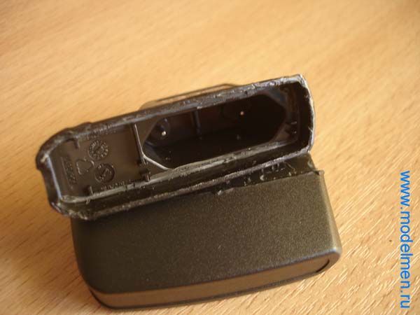
To start the block you need to disassemble. Judging by the seams on the case, this unit is not intended for disassembly, hence the thing is disposable and large hopes in the event of a breakdown can not be placed.

I had to get the charger body in the literal sense, it consists of two tightly glued parts.

Inside the primitive fee and several parts. Interestingly, the fee is not soldered to a 220V fork., And attached to it with a pair of contacts. In rare cases, these contacts may oxidize and lose contact, and you think that the block broke. But the thickness of the wires going to the connector on the mobile phone was pleasantly pleased, do not often meet the normal wire in one-time devices, it is usually so thin that even touching it is scary).

On the back of the board turned out to be a few details, the scheme was not so simple, but still it is not so complicated, so as not to repair it on its own.

Below in the photo contacts of the granddaughter of the case.
In the charger diagram there is no lowering transformer, a regular resistor plays his role. Further, as usual, a couple of straightening diodes, a pair of capacitors for straightening the current, after the throttle is going on and finally the stabilion with the capacitor is completed with the chain and remove the reduced voltage to the wire with the connector to the mobile phone.

In the connector only two contacts.

Now all manufacturers of cell phones have already agreed and everything that is in stores is charged via a USB connector. It is very good, because the chargers have become universal. In principle, the charger for the cell phone is not.
This is only a pulsed direct current source with a voltage of 5V, and the actual charger, that is, the diagram of the battery charge, and ensures its charge, is in the cell phone itself. But, the essence is not in this, but in the fact that these "charging devices" are now sold everywhere and are so cheap, that the issue with repair disappears somehow by itself.
For example, in the store "Charging" costs from 200 rubles, and on the famous alikexpress there are offers and from 60 rubles (including delivery).
Schematic scheme
A typical Chinese charging circuit, drawn from the board, is shown in Fig. 1. There may be a variant with the permutation of VD1, VD3 diodes and VD4 stabilodon on a negative chain - Fig.2.
And more "advanced" options can be rectifying bridges at the inlet and outlet. There may be differences in the nominal details. By the way, the numbering in the schemes is given arbitrarily. But the essence of the matter does not change.
Fig. 1. Typical scheme of a Chinese network charger for a cell phone.
Despite the simplicity, it is still a good pulse power supply, and even stabilized, which is quite good and to power something else, except for a cell phone charger.

Fig. 2. Scheme of a network charger for a cell phone with a changed position of the diode and stabilion.
The scheme is made on the basis of a high-voltage block generator, the latitude of the generation pulses of which is adjusted using the optocoupler, the LED of which receives the voltage from the secondary rectifier. Optopara lowers the offset voltage on the basis of the key transistor VT1, which is set by resistors R1 and R2.
The load of the transistor VT1 is the primary winding of the T1 transformer. The secondary, downward, is the winding 2, with which the output voltage is removed. There is still a winding 3, it also serves to create a positive feedback for generation, and both for a negative voltage source, which is made on the VD2 diode and C3 condenser.
This negative voltage source is needed to reduce voltage based on the transistor VT1 when the U1 optocouple opens. An element of stabilization determining the output voltage is the VD4 stabilion.
Its stabilization voltage is such that in the amount with direct voltage of the IR LED, the optocouplers U1 gives exactly the most necessary 5V, which are required. As soon as the voltage on C4 exceeds 5V, the VD4 stabilitron opens and current through the optocouples LED through it.
And so, the work of the device of questions does not cause. But what to do if I need not 5V, but, for example, 9v or even 12v? The question arose together with the desire to organize a power supply unit for a multimeter. As you know, popular in amateur circles, multimeters are powered by "crowns", - compact battery with voltage 9V.
And in the "hiking" conditions, this is quite convenient, but in domestic or laboratory, I would like nutrition from the mains. According to the scheme, "charging" from the cell phone in principle is suitable, it has a transformer, and the secondary chain does not contact with the power grid. The problem is only in supply voltage, the "charging" gives 5V, and the multimeter needs 9V.
In fact, the problem with an increase in the output voltage is solved very simply. You just need to replace the VD4 stabilitron. To get a voltage suitable for powering a multimeter, you need to put a stabilion to a standard voltage of 7.5V or 8.2V. At the same time, the output voltage will, in the first case, about 8.6V, and in the second about 9, sv, that, both, and the other is quite suitable for the multimeter. Stabilirt, for example, 1N4737 (this is 7.5V) or 1N4738 (this is 8.2V).
However, you can and another low-power stabilion on this voltage.
Tests showed a good operation of the multimeter when eating from such a power source. In addition, an old pocket radio receiver was also tried from "Crowns", - worked, only interference from the power supply slightly interfered. Voltage in the 9V case is not completely limited.

Fig. 3. Voltage adjustment node for alteration of the Chinese charger.
Want 12V? - Not a problem! We put Stabilitron at 11V, for example, 1N4741. Only you need C4 capacitor to replace the highest voltage, at least 16V. You can get even more tension. If the stabilion is completely removed at all, there will be a constant voltage of about 20V, but it will not be stabilized.
You can even make an adjustable power supply, if the stabilion is replaced by an adjustable stabilion, such as TL431 (Fig. 3). The output voltage can be adjusted, in this case, the R4 variable resistor.
Karavkin V. RK-2017-05.